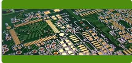
Manufacturing and Technical Questions
Q01: Does Yashna Circuits bevel gold fingers?
Q02: What is your standard bevel on a printed circuit board?
Q03: What is tab route?
Q04: What does "scoring" mean?
Q05: What is the difference between proto and production?
Q06: What files do you need to manufacture my printed circuit board?
Q07: What do you need if I want my pcb penalized in array format?
Q08: Do I have to have my printed circuit board electrically tested?
A01:Yes. We do bevel gold fingers unless otherwise specified. We do NOT bevel solder fingers unless specified by customer.
Back
A02: Our standard bevel is 30 degrees leaving a .030" edge (+/-.005") on a .062" board. Optional bevels are as follows:
45 degrees leaving .025" edge (+/-.005")
20 degrees leaving .071" edge (+/-.005")
Back
A03: A tab route is used to create arrays, often called "route and retain". The customer can place more than one board (same or different design) up in a given area in an array or penalized configuration. This is typically for the convenience of the customer or for assembly requirements that utilize pick and place machines to load components. The PCB's are then separated by breaking or cutting the tabs. Tabs are usually 0.100" in width and are placed with at least 1 on each side of the boards.
Back
A04: This is a "v" groove cut into the top and bottom surface of an array of multiple PCB's or between a board and rails to be removed after assembly. The cut is usually 1/3 top, 1/3 bottom, leaving 1/3 uncut in the middle. This process is used when removing the tabs of a tab route is not a viable option, this does result in a less smooth finished board edge. The boards are typically set up side by side and end to end with the edges adjacent to each other. After assembly the boards are broken or snapped apart.
Back
A05: The difference between proto & production is not a quantity or turn time issue, but rather has to do with the range of specs covered. Click here for a complete list of these specifications.
Back
A06: We prefer gerber files (274X or 274D with an aperture list), an excellon drill file, and a drill tool list (may be included in excellon drill file). We can use other formats such AutoCAD dxf to create gerbers for you. Please send any non-gerber formats.
Back
A07: We recommend you send us your complete array pre-panelized. This allows you to set up the array exactly the way you want it. If you need us to set up your array, please be aware that additional engineering time may be billed.
Back
A08: Electrical testing of your printed circuit boards is certainly not required. However, the more complex the product the higher the probability that it may suffer defects that could affect the electrical characteristics of the board.but which could not be detected from visual inspection alone. There are a large number of variables that affect the decision to test a board such as layer count and complexity of design, criticality of potential time loss for project, and expense of components to be loaded.
Back
|