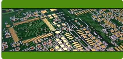
Blind & Buried PCB
Technical specifications for Multilayer PCB's
 | |  |
 |
Capability | Standard |
|
| Board types | Multilayer up to 10 Layers | Board Profiling | CNC Rout |
| Score |
| Pierce Blank & Return | Minimum PWB trace width | 5 mil ( 0.127 mm ) | Minimum Track Width to feature spacing | 5 mil ( 0.127 mm ) | Smallest drilled hole | 0.4 mm | Material Thickness | 0.4 mm - 3.2 mm | Copper Thickness | Up to 6 oz Cu | Max board size | 600 mm x 450mm | Standard Surface finish | Hot Air Solder Level | Alternative finishes | Electroless Nickel / Immersion Gold |
| Rohs |
| Electroless Tin Lead |
| Carbon |
| Hard Gold ( edge contact ) |
| Peelable | Bare Board Test | Bed of Nails |
| Double-sided flying probe test | Solder mask | Photoimageable Resist with green, red,black,white & yellow colors . | Gold plate | Edge connectors Touch Pads | |
 |
 | |  |
© Copyright 2008 yashnacircuits.com
Website developed & maintained by
|